Building a Crank & Cam Simulator
For some of the work I have been doing on K Series ECUs and immobilisers I needed to be able to “run” an ECU on the bench. Rather than just powering the ECU I needed to be able to make it think it was running the engine, firing the fuel injection and ignition systems. My immediate requirements were to be able to:
· Dead/Alive test ECUs that I’d been hacking around with internally.
· Test the immobilisation status of an ECU/Immobiliser set. I will write up separately the work I’ve done on a key programming and ECU and immobiliser testing interface, but the process of matching the MEMS3 ECU to the 5AS immobiliser is occasionally a bit hit and miss. Occasionally the ECU reports that it has learned the security code but still fails to recognise the immobiliser and need programming again. I needed to be able to detect this on the bench, and the only way I could think of was to get the ECU into a running state and see if it continued to run indefinitely.
However, being able to run an ECU on the bench and off the car would have helped me investigate and diagnose a number of issues that I’ve looked into in the past, and being able to run the ECU on the car but without actually running the engine would also be a very useful diagnostic tool.
I reasoned that the only thing the ECU really needed to get it running was a crank sensor signal, and to get it running “properly” with sequential injection etc. for testing purposes would also require a cam sensor signal. But the crank sensor signal is quite complex given that the flywheel has a specific pattern of missing teeth which the ECU needs to be able to synchronise to and the cam sensor signal is also a bit complex, being quite different on a VVC engine (variable reluctance sensor like the crank sensor, two trigger teeth on one inlet cam reading both cam phase and cam duration, analogue signal) and the non-VVC engine (powered Hall effect sensor providing a 50% duty cycle square wave, cam phase only digital signal).
I therefore set about designing and building a crank and cam simulator.
I hooked up an oscilloscope and captured the signals with the engine at idle (which was all I really needed to be able to simulate). I was quite surprised by the voltage generated by the crank sensor, it was about 10V peak to peak at idle and because it generates a voltage which is proportional to the rate of change of the magnetic flux, the voltage as well as the frequency increased in proportion to engine RPM. At the redline it is generating around 70V!
Once I had the oscilloscope traces, I set about fitting some mathematical curves to the different parts of the waveforms until I had a mathematical model which was a close approximation to the whole engine cycle (two complete crank revolutions).
As an aside, I’m pretty sure that the ECU actually just detects the points where the voltage crosses through zero volts from positive to negative for the crank and VVC cam sensors; if you mark these points out on the waveform you actually get the exact pattern of teeth on the trigger wheels, completely independent of the amplitude of the signal, with one point at the centre of each tooth and missed point where a tooth is missing (you get positive voltage as the magnetic flux ins increasing, i.e. as the sensor is coming onto a tooth, a negative voltage as the magnetic flux is decreasing, i.e. as the sensor is moving off a tooth, and the switch between the two occurs exactly at the centre of the tooth where the flux is neither increasing not decreasing). So in reality I could probably have stimulated the ECU correctly with a simpler signal pattern than the one actually produced by the sensor. But I really wanted to generate a realistic signal as this would be a lot more useful for diagnostic purposes.
Having worked out some functions which gave me a good match, I then resampled the functions I had come up with at 8192 points (I wrote a little program to generate the data files), rounding each one to 8 bits accuracy, i.e. 256 voltage levels between the lowest and highest voltage points in the waveform. My plan was to load these 8192 points into two ROM chips and use a simple oscillator and counter to cycle round the 8K addresses. The data lines from the ROMs would then be fed to two digital to analogue converters to recreate the voltage waveforms.
After a bit of breadboard prototyping and messing around, this is the circuit I came up with:
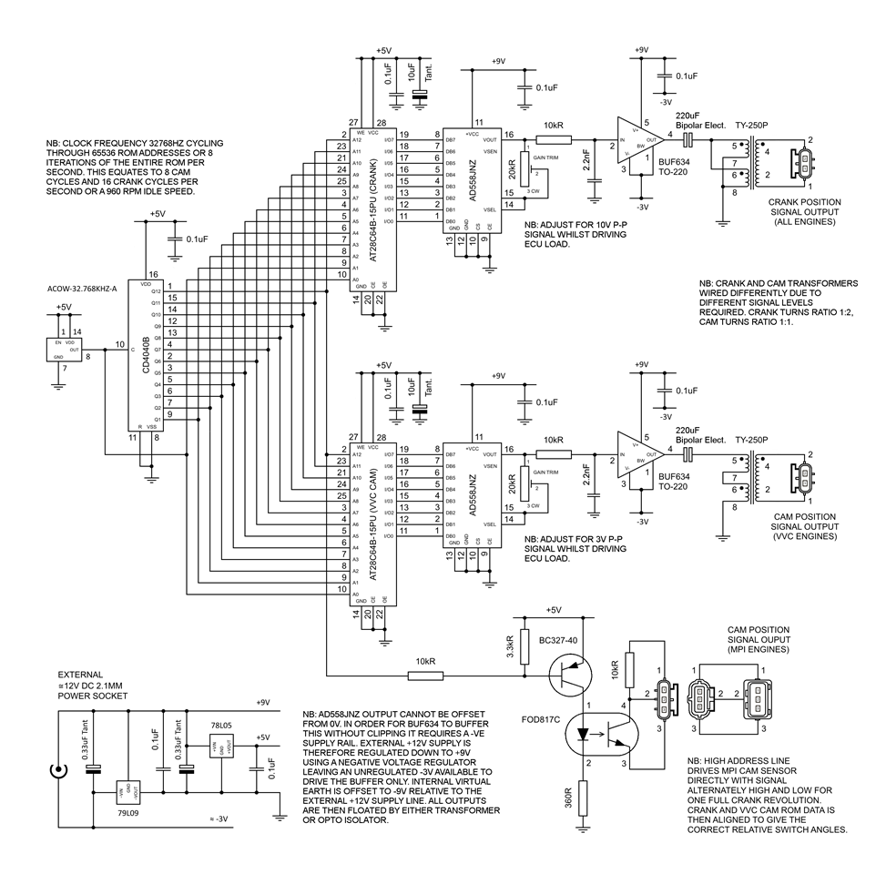
I used a standard 32768hz (a common frequency, if you divide it down with a binary counter 15 times you get 1 cycle per second) clock oscillator module (ACOW-32.768KHZ-A), driving a CD4040B 12-stage binary counter. This actually counts through 65536 addresses per second, as each cycle of the clock has a “low” part and a “high” part, so two addresses per one cycle of the clock. This means it counts through the 8192 addresses of the ROM chips 8 times per second, so simulates 8 complete engine cycles per second. Each engine cycle is two crank revolutions, so it simulates the engine running 16 revolutions per second or 960rpm, which is a reasonable approximation to a cold idle.
The two 28C64 ROM chips are loaded with the data obtained from digitising the waveform functions. The data lines are fed directly to AD558 digital to analogue converters. I wanted to simulate the digital output signal of the non-VVC cam sensor too. The easiest way to do this was to just use the high order address line directly, which was high for one crank revolutions and then low for one crank revolution. In order to have this signal switch at the correct point in the cycle, I offset the data in ROMs to align the crank and VVC cam signals with the non-VVC cam signal, rather than the other way around.
This approach of counting through the ROMs lead to a few difficulties.
· As each stage of the counter drives the next, the address lines don’t switch at exactly the same time. This and the internal workings of the ROM chips mean that intermediate states are accessed very briefly as the addresses switch over from one count to the next. In this simple design the memory chips are permanently enabled, so these transient addresses meant that the output tended to have short sharp spikes superimposed on the waveform. However these were extremely short duration and I was always going to have to add a filter stage to smooth the stepped digital output into a nice smooth analogue signal again. The 10kR resistors and 2.2nF capacitors at the outputs of the converters performed both filtering tasks very effectively.
· The analogue to digital converter outputs could not be offset from zero; the range was always 0V to some maximum voltage. I wanted to drive the very impedance outputs into a buffer amplifier stage and in order for this to be able to operate right down to 0V without clipping I needed a negative supply voltage, below ground. For this reason I used the rather odd power supply arrangement shown. I used a -9V regulator (79L09) hanging off the external +12V line to split the 12V supply into an internal virtual ground, with +9V and -3V supplies. The -3V was adequate to driver the buffers. I then further regulated the internal +9V down to +5V for the digital logic. This meant that the internal and external grounds were at different levels, which could have been a problem when operating it off the vehicle supply; however as I had already decided that I wanted the outputs to appear to the ECU exactly like actual sensors, which are generally completely isolated floating voltage sources, I was planning to fully isolate them anyway which meant the internal ground level would never be exposed.
· The analogue to digital converters supported only fixed 0-2.55V or 0-10V ranges by connecting different combinations of pins together. I wanted to use a unity gain output buffer as I had problems with noise using operational amplifiers with higher gains (the digital side of the circuit generates a lot of noise and using simple stripboard construction techniques it is hard to stop this coupling into the analogue signal - using a unity gain buffer chip meant that the feedback was all tightly internal to the chip and a lot less susceptible to noise issues). This meant that I needed to be able to adjust the voltage range of the converters. After studying the datasheet, it seemed that the reason that only these two fixed ranges were supported is because resistors internal to the chip are used in the gain setting network and while these are very precisely matched to each other during manufacture, they did not have guaranteed precise absolute values (I think they are laser trimmed during to production to raise the resistances of those which are too low to match the highest, whatever that happens to end up at), so even using precision external resistors to adjust the gain the results may vary quite a bit due to the differences in internal resistances between devices. From this I worked out how to use external resistors to get the gains I needed; in this application the exact amplitude of the signal wasn’t so critical and I included 20kR trimmer preset potentiometers in the design to allow the gain to be adjusted as required.
After that I used BUF634 buffer amplifiers to drive TY-250P signal transformers, which provided the required isolation of the outputs. The gains used for the converters and the wiring of the transformers are slightly different between the cam and crank stages to obtain the desired voltage levels to match those seen on the car; around 10V peak to peak for the crank signal and 3V peak to peak for the cam signal.
I used an optical isolator stage for the non-VVC cam sensor signal.
This resulted in the outputs for the crank and VVC cam stages being floating wire coils (the transformer secondaries, emulating the coil windings of the actual sensors) and the output of the non-VVC cam stage is an isolated saturated transistor switch to ground, again emulating the output circuit of the actual sensor. There is complete isolation between all of the outputs and between the outputs and the power supplies. This means that the offset internal virtual ground becomes irrelevant.
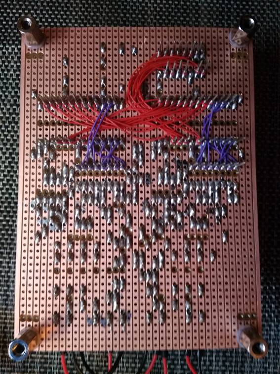
For ease of construction I decided upon a simple stripboard design using good old fashioned wire wrapping in Kynar wire for the digital address and data buses.
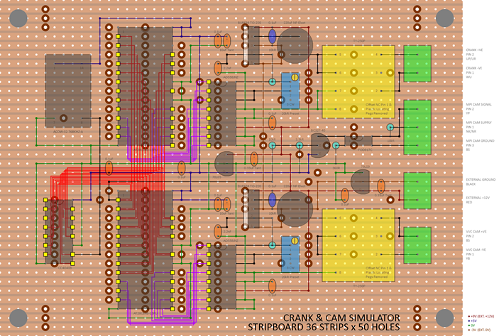
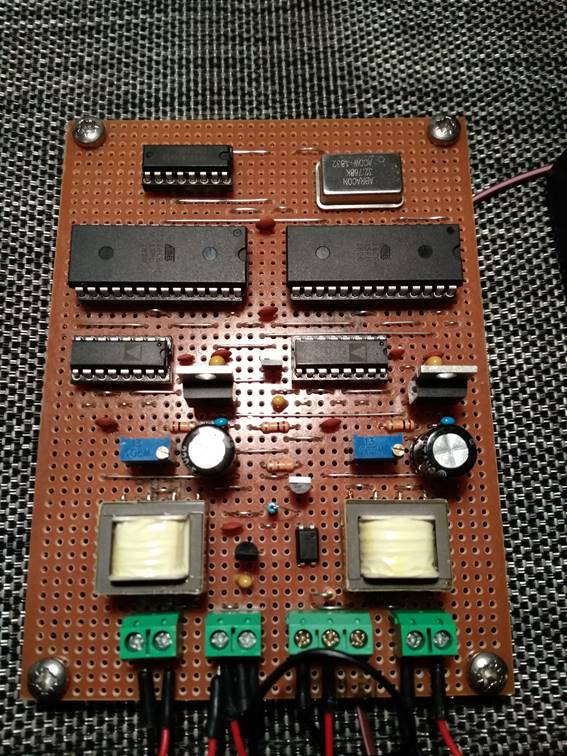
Below are pictures of the finished circuit board:
And here is the overall construction of the unit in its case:
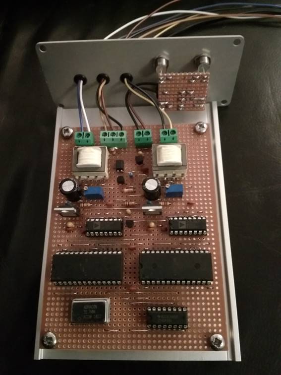
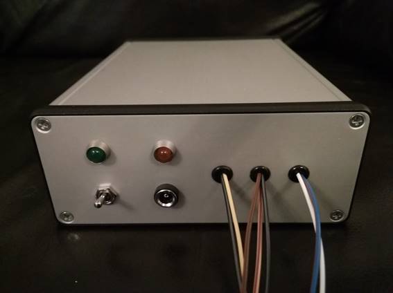
The cables lead to appropriate male connectors which plug into the female wiring loom connectors. The orange LED indicates when there is power supplied to the 2.1mm DC socket, the green LED indicates when the unit is switched on and generating signals.
And here are some oscilloscope traces of the signal waveforms produced at different time resolutions. The green traces are the crank signals, the yellow traces are the cam signals. I’ve not included the non-VVC cam signal here as my scope only has two channels and it’s not so interesting anyway, being just a digital square wave switching between the voltages of the external supply provided:
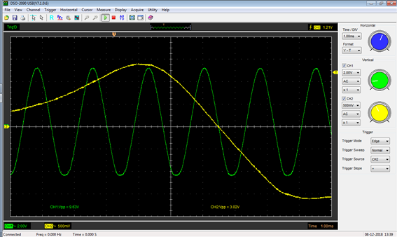
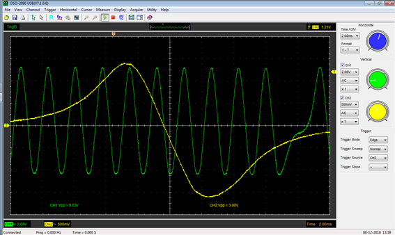
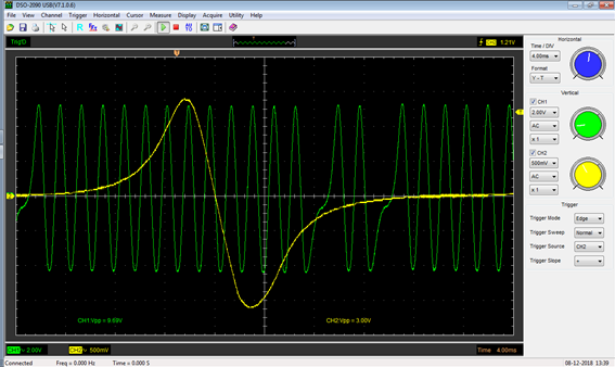
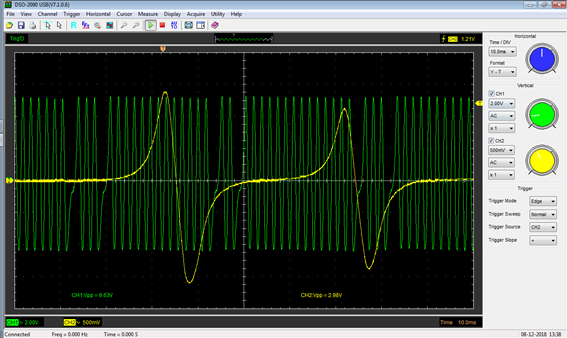
In the last picture the missing teeth in the crank waveform can clearly be seen.
Despite my best efforts there is still a little bit of digital noise breakthrough on the analogue waveforms but it is in the millivolt range and they are certainly acceptable and in reality much less noisy than the real signals on a running engine (and it is actually rather less noisy that it appears in the pictures above as most of the noise visible in the pictures is just the limitations of the scope used, which shows a similar noise level when the input is grounded).
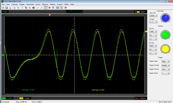
The picture below shows how the simple resistor and capacitor filter is effectively smoothing the output of the analogue to digital converter. The green signal is the raw output and the sharp switching transients can be clearly seen. The yellow signal is the final output, with both the spikes and the quantization steps smoothed out. This picture also demonstrates that the odd power supply arrangement is working and there is no clipping of the waveform at the extreme peaks or troughs (the green and yellow signals don’t follow each other exactly simply because of the gains through the circuit and the fact that I had to choose the nearest fixed voltage scales on the scope to get them as close as possible, but you can see that the shapes of the two waveforms follow each other fairly closely).
And does it actually work …
Well, if I feed the crank signal to an ECU powered up on the bench, it immediately turns on the fuel pump signal and starts firing the ignition and injection circuits. This means it must have correctly recognised the tooth pattern in the crank signal and has correctly synchronised to the position of the simulated flywheel. Initially the injectors all pulse together, but as soon as I also feed the cam signal, it switches to fully sequential injection mode, pulsing the injectors in 1-3-4-2 firing order.
I’ve already used this to learn quite a lot of interesting (in a very geeky way!) things out the workings of the ECU. Things like what exactly does control the fuel pump drive (it’s certainly not the immobiliser as is often stated), what exactly does the immobiliser shut down, and is the ECU essentially digital or analogue (it’s a lot more analogue than I at first assumed). I will write these up separately when I do a post about the key programming and ECU testing harness that I’ve made up, including videos if it all running where you can clearly see the injector patterns etc.
Although I designed this specifically for use with the K Series, it would probably only require minor adaptation to be used with other engine types, ECUs and flywheel patterns.
PS: If anyone would
find any of this interesting or useful I have all of the plans, design
calculations, waveforms, data files, mathematical models etc. saved away and
happy to share.