Decoding & Cloning The Lucas 5AS Immobiliser - Part 1
So for my next challenge…
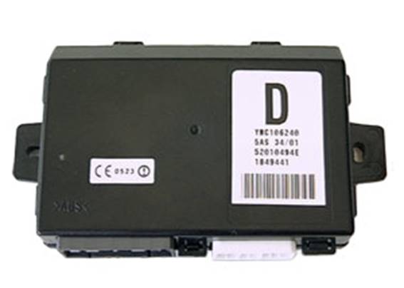
Not my photograph -
https://blackbox-solutions.com/help/SM034_ecu.jpg
The Lucas 5AS Immobiliser as used with the K Series engine comes in a number of different flavours. With the correct tools it is highly configurable. However, other than for matching remote key fobs and changing the EKA code, the tools with are able to configure the 5AS are generally very expensive and very hard to come by, e.g. the Rover Testbook T4 system. These are beyond the reach of individual owners wishing simply to change configuration settings.
The immobiliser in my car is configured for passive arming. After a period of approximately 10 minutes has elapsed after turning off the ignition switch, the immobiliser arms itself automatically. The alarm functionality of the 5AS does not arm unless manually armed by the key fob, but the engine is immobilised. I planned to do some modifications to implement the alarm functionality which is not generally present in a Caterham and for this it was important for me to retain the passive arming of the immobiliser and I was happy with the way it was configured.
I have a few spare immobiliser units, mostly picked up cheap on eBay with unknown histories and from unknown donor cars, with a variety of different configurations, some of which do arm passively and some which do not. They all arm after a few seconds of turning off the ignition switch and the opening and closing the driver’s door (in a Rover! I tested this functionality by wiring up a mock door switch) but the passive arming in a Caterham setup was inconsistent. They also displayed quite a range of different behaviours in terms of the dash LED signalling, how they responded when the key fob battery was getting low (some gave a visual warning by flashing the LED rapidly, some did not, and some required two presses of the key fob each time to bring the low battery to the attention of the user, some did not). Ideally I would like to modify or configure all of the spare immobilisers to work exactly like the one in my car as spares as I was completely happy with all of the settings and behaviours of this one. But as described above, there is no easy way to access the settings.
One possibility would be to access the EEPROM memory (non-volatile memory inside the microcontroller chip in the immobiliser) directly. The main problem with this approach is simply that there is simply no way for me to know which memory addresses correspond to which settings and how the values for the various configuration settings are stored. What I could do though would be to copy the entire EEPROM contents across from one immobiliser to another, hopefully transferring all settings without having to understand them. However, this would mean that all of my immobilisers would probably then have the same “unique” MEMS codes and “secret” EKA codes. Now this could be seen as an advantage as I would be able to swap immobilisers without having to code them into the ECU again, but if I were ever to sell one or do the same modifications for somebody else, I wouldn’t want to be handing out immobilisers which would run my car without coding, and since I have key programming tools which make it easy to code an immobiliser into an ECU I really wanted to do it properly - copy all settings but preserve the original serial number and MEMS and EKA codes. The serial number is printed on the label of the 5AS so should be easy enough to find in the EEPROM data and the EKA code is readable with a key programmer but the MEMS code is only accessible through the coded signal sent to the MEMS3 ECU. Other than by attempting to decode this signal, there is no easy way that I know of to know what the MEMS code for a given immobiliser is and therefore no way to know what to look for in the EEPROM data.
Now at this point you may be wondering why I don’t just take a spare immobiliser to somebody who has a T4 and can reprogram it for me and give him £25? Well I have to admit that part of it is just that I like a challenge, and the tougher the better. But I firmly believe that the more we can as a community understand and document the systems on our cars, the better we will be able to support them in the longer term when the experts have packed up and gone home. There is precious little information out there on the web at the moment about the detailed working of the standard engine management and immobiliser systems on the K Series. For my liking there are far too many cases on the various Rover forums where questions about particular systems just come to the conclusion that “X is your man”, and X happily fixes things for a wad of cash and keeps the information on how he did it very close to his chest indeed. I would much rather know how to produce a spare immobiliser to the required specification at will than just have a spare immobiliser of the required specification.
Hacking these systems is always a bit like trying to get the cellophane wrapper off a CD … once you’ve got one edge up it’s a lot easier to get the rest off.
So I set about the challenge of cracking the encoding of the signals passed from the 5AS immobiliser to the MEMS3 ECU from first principles. From what I can see, the signal encoding is identical for all 5AS units and all generations of Rover MEMS engine management. My test cases include six 5AS immobilisers and an assortment of MEMS3 ECUs, mostly VVC 160 but also Rover 214 and 216.
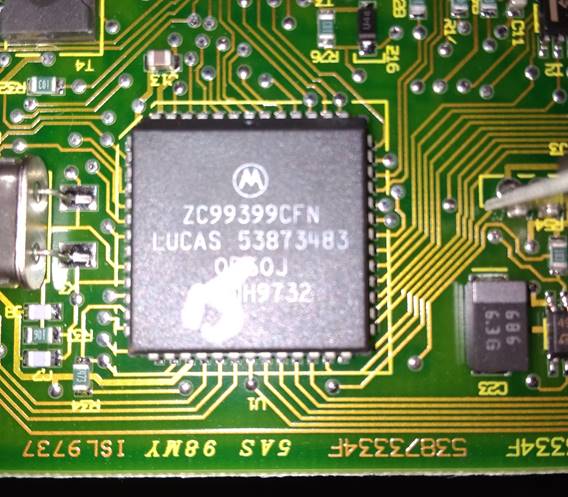
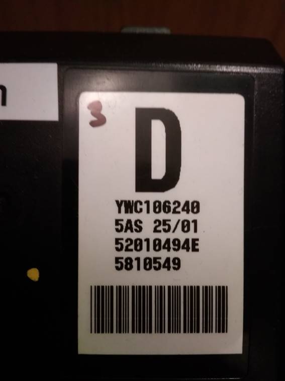
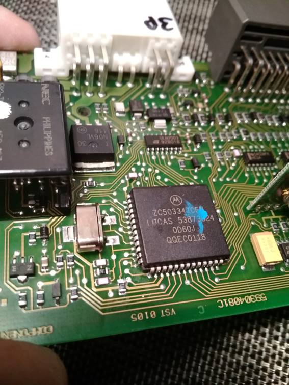
From the sample I have here, and from one or two others I’ve looked at, the 5AS immobiliser comes in two major flavours. The later ones are referred to as “98MY”. My guess would be that this refers to “Model Year” but I have one 98MY unit with a date code of 28/96 (Week 28, 1996) stamped on the front label and an earlier non-98MY unit with a date code of 39/97, so I’m really not sure how the transition between the two occurred. All of those with date codes later than 1998 seem to be reliably 98MY variants. As far as I can tell, all of the later 98MY immobilisers are for all practical purposes identical from a hardware perspective. All of my 98MY immobilisers had a part number of YWC106240 but I’m sure there are other part numbers which differ only in configuration. The circuit boards seem only to differ in cosmetic ways and the only variations I have seen in the components mounted on the board look to be just variations between different suppliers of essentially the same generic components. The pre-98MY immobilisers seem to show more variation. Very early units only had a single connector socket, but even between dual socket units I can see variations in the exact microcontroller chip used, with different part numbers and mask codes. The microcontroller chips on all 98MY immobilisers that I have seen have been Motorola ZC503347CFN, stamped with Lucas 53873824 and a mask code of 0D60J.
For these reasons, I have decided to focus on the 98MY immobilisers. I am reasonably confident at this point that the EEPROM contents should be transferable between units and should work properly with any firmware and hardware on the new unit. The message decoding work I have documented below is applicable to all variants, but I’m only going to try to transfer EEPROM settings between 98MY variants.
Research on the Internet identifies the ZC503347CFN microcontroller used as a Motorola MC68HC05B16. The mask code 0D60J refers to the minor revision (I believe that minor revisions were made to the chip designs to fix issues, and that the detailed hardware behaviour may vary slightly in certain documented cases between processors with different mask codes). These are very much a “Computer on a Chip” and the 5AS circuit board contains little else other than some generic HC logic “glue”, ULN2003 driver chips, power supply circuitry, the radio receiver module and various bits that look to be associated with driving external circuits, such as a large power MOSFET, some power diodes and a couple of relays. There do not appear to be any other programmable memory elements so all settings must be stored within the microcontroller in the internal EEPROM.
The MC68HC05B16 contains mask-programmed ROM, which is basically memory which is pre-programmed as part of the design and manufacturing process and cannot subsequently be modified. My assumption is that the “Lucas 53873824” stamping on the chip identifies the ROM program which will have been developed by Lucas and supplied to Motorola for programming during manufacture. I’m hoping that as all of my immobilisers are stamped “Lucas 53873824”, the programming will be identical and therefore the EEPROM contents will be compatible.
The MC68HC05B16 also has a built in security mechanism to protect the internal memory contents from external access using programmers etc. Being a complete “Computer on a Chip”, there is no need for the internal data to be externally accessible in normal operation; the code on the device supports external programming of options and settings as required through communications interfaces and does not make the internal storage of these available. The microcontroller can operate normally in “user mode” or be switched into “non-user” or “test” mode, which allows access to the internals. There is one bit in the first byte of the EEPROM memory which, when set, prevents the microcontroller from switching to “non-user” mode. This is designed to prevent the use of universal programmers to access the data. The idea is that the only way to reset this bit is to erase the memory, which also erases the protected data.
However, over time hardware issues have been discovered which allow certain techniques to bypass this security. The MC68HC05B16 has been found to be vulnerable to clock glitching and other fault injection attacks. These involve running the system clock, voltages or other parameters out of specification for a very short period at critical times to cause the processor to miss-execute a particular instruction, exploiting oddities in the internal timing as different transistors within the chip switch. Using such techniques it is possible to trick the microcontroller into switching into “non-user” mode even when the security bit is set. Some universal programmers such as the XPROG-M (and cheap Chinese clones of these) are able to exploit these vulnerabilities to both read and write the protected memory. With these programmers, the processes require to bypass the security are fully automated and routine, and the programmers allow access to the internal contents of secured chips almost as though there was no security implemented.
So my overall plan of attack at this stage is:
· Open up the case.
· Record the communications between the 5AS and MEMS3 using a digital storage oscilloscope.
· Figure out how to decode this to discover the unique MEMS codes for my immobilisers.
· Desolder the microcontroller and mount it in an XPROG-M programmer.
· Bypass the microcontroller security to read the EEPROM data and save it as a .BIN (raw binary) file.
· Find locations used for the MEMS code, EKA code and serial number in the EEPROM data.
· Do the same for another 5AS box.
· Update the data read from the first 5AS with the MEMS code, EKA code and serial number from the second 5AS.
· Write the modified data to the second 5AS microcontroller.
· Solder the microcontroller back into the second 5AS.
· Hopefully the second 5AS will then retain its unique IDs but have all of the settings of the first.
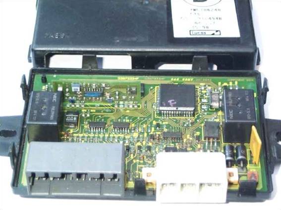
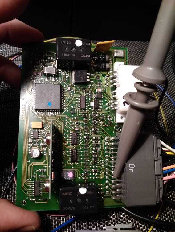
Opening the case up was easier than it looked. There are 8 plastic clips around the edge and I thought it might be awkward to release them all at the same time, but in reality the case is flexible enough to allow you to release the clips at one end and then hold them slightly apart as you work down the sides until the case comes apart. I released each clip simply by slipping a small flat screwdriver into the clip to depress the latching tongue.
Not my photograph -
https://www.mgfcar.de/alarm_blipper/dcp_1556.jpg
The only information I really knew about the MEMS code was that it was 16 bits in size, from sites such as this: https://blackbox-solutions.com/help/SM034.html (I have since had it that the code is 16 bits in size, that any code other than 0x0000, 0xFFFF and 0xF0F0 is valid and the transmission rate is 125 bits per second).
So I connected an oscilloscope to Pin 9 of the immobiliser to record the communications between the 5AS and the ECU. All of this work was done with an immobiliser and an ECU connected to a test wiring harness on the bench for convenience but could equally be done in situ with the immobiliser plugged into the car wiring loom.
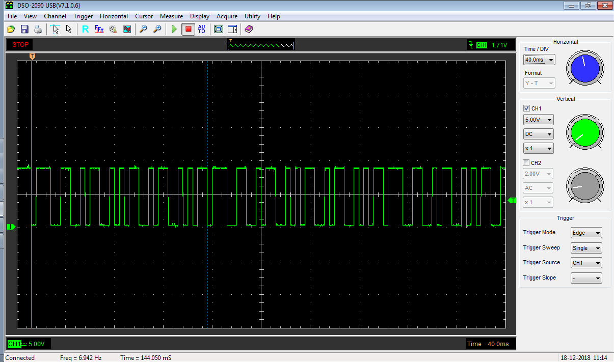
The result was clearly a digital signal, switching between a high “1” and a low “0” voltage. Initially it appeared to be just a constant data stream with no obvious beginning or end to the messages, so to make life a little easier on myself I turned off the ignition, set the oscilloscope to trigger on the voltage falling though a voltage midway between the two levels and to capture a single sweep, then turned on the ignition. The oscilloscope then captured the very first part of the communication - which I guessed represented the start of the first message. The captured waveform was as shown below. The “T” indicator at the top of the display is the trigger point. With the ignition turned off, a continuous “1” was transmitted. The trigger point is the point where the voltage first switched to a “0” and represents the start of the first message.
I repeated this same procedure for the six immobilisers I had to hand, and collated the waveforms as shown below, in order to look for patterns. So, what could I learn from these six waveforms?
The first thing I noticed was that they clearly all consisted of a number of “bits” of equal duration. I added the red lines in the picture below as an equally spaced grid using the Paint.NET image editor. They correspond to approximately 4ms time intervals and you can see that the transitions between the “1” and “0” levels all take place at these fixed intervals. This was the clock signal recovered from the waveform.
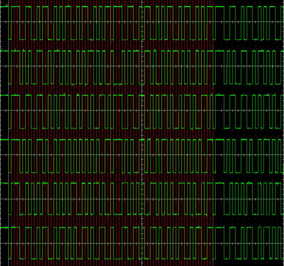
The second thing I noticed was that the different signals all started off in the same way, with the first 4 bits of the sequence being “0111”. This looked like some sort of message header (actually the first 5 bits of the sequence were always “01110”, but I’ll come back to that later). After that the patterns differed.
The third thing I noticed was that each of the patterns repeated after a period of time. So it didn’t look like any kind of two way conversation between the 5AS and the ECU, just a repeated broadcast of the same message by the 5AS over and over again. And there obviously wasn’t any attempt to obfuscate the message using some kind of rolling encoding (which would mean that subsequent transmissions of the same message content were encoded differently, as is done for example with remote key fobs to foil code-sniffing attacks). So I was left with the challenge of simply decoding the formatting of the message content and the encoding scheme used.
The fourth thing I noticed was that, although the first bit of each message was always a “0”, the last bit could either be a “0” or a “1”. Now I had been expecting find a standard UART-type serial signal, with “start bits” of one type and “stop bits” of the other - basically the line would sit at one level, presumably the high 5V level in this case as that is what I saw before the start of the first message, for a minimum of a set number of bit periods at the end of one message before switching to the other level to signal the start of the next message. In this case, other than being able to determine the start of the message by capturing the first transition after switching on the ignition, there was no obvious way for the ECU to break the data stream into messages.
The next thing that struck me as strange at first was that the repeat periods for the different immobilisers differed. Some patterns repeated every 36 bits, some repeated every 72 bits. This difference didn’t seem to correlate with any differences in the versions of the immobiliser or anything else I could see. One closer inspection I spotted something rather curious. In those patterns which repeated every 72 bits, the last 36 bits of the pattern were in fact simply a repeat of the first 36 bits, but inverted. So every time a “0” appeared in the first set of 36 bits, a “1” appeared in the second set of 36 bits. The last 36 bits of the pattern therefore contained no new information, and in fact the information content was repeating every 36 bits for all immobilisers, just some of them were inverting every second transmission of the message and some were not.
The repeated sequences generated by the six immobilisers are show below:
Immobiliser 1:
011100110010110010101100101100101011011100110010110010101100101100101011
Immobiliser 2:
011101010011001011010100101011010100100010101100110100101011010100101011
Immobiliser 3:
011100110011001010110100101101001101011100110011001010110100101101001101
Immobiliser 4:
011101010011010010110101010101010011011101010011010010110101010101010011
Immobiliser 5:
011100101010110010101011001010110100100011010101001101010100110101001011
Immobiliser 6:
011100110010110010110101001101001100100011001101001101001010110010110011
This set me thinking, and I realised that the only way it made sense was if the information was encoded in the transitions between levels, and not in the levels themselves. So the actual logical “1”s and “0” could be represented by “switch” or “no switch” between the levels at each clock point, rather than by the high and low voltages themselves. This would mean that for a message with an even number of transitions, the voltage at the end of the message would be the same as the voltage at the start of the message, so the second message would be starting from the same level and would be exactly the same as the first. For a message with an odd number of transitions, the voltage at the end of the message would be the inverse of the voltage at the start of the message, so the second message would be an inverted copy of the first message, the third would be the same as the first etc. This is exactly what I was seeing.
This rang a distant bell in my memory and a bit of digging on the Internet brought up the specification for NRZ-S line-encoding, often used in telecommunications. This is “Non Return to Zero, Space” encoding. “Non Return to Zero” means simply that the voltage doesn’t return to the “0” state between bits, it just switches directly between the “0” and “1” states. This has the disadvantage that, for long runs of consecutive “0”s or “1”s there are no transitions and therefore no clock signal - then sending and receiving clocks can get out of step. The “Space” part means exactly what I had worked out above - a “0” is encoded by switching between levels and a “1” is encoded by remaining at the same level at each clock interval. In this case, long runs of “0”s cause the signal to switch at every clock point which means the receiver is still able to remain synchronised to the transmitter’s clock, however long runs of “1”s still result in no transitions. In order to get around this, it is normal to insert some “0”s into the transmitted data stream according to some predefined pattern. NB: There is an alternative encoding called NRZ-M, or “Non Return to Zero, Mark” which is identical except that transitions occur for “1”s rather than “0”s. At this point I have no way of distinguishing which of these encodings may be used here, which is something I will need to bear in mind when trying to find the decoded bytes in the EEPROM data.
So it looked as though the messages being transmitted by the 5AS were 36 bit NRZ-S encoded, so the next thing I did was to decode the line-encoding to see the underlying byte streams being transmitted:
Immobiliser 1:
001101010100010100000101000101000001 001101010100010100000101000101000001
Immobiliser 2:
001100000101010001000001000001000001 001100000101010001000001000001000001
Immobiliser 3:
001101010101010000010001000100010100 001101010101010000010001000100010100
Immobiliser 4:
001100000101000100010000000000000101 001100000101000100010000000000000101
Immobiliser 5:
001101000000010100000001010000010001 001101000000010100000001010000010001
Immobiliser 6:
001101010100010100010000010100010101 001101010100010100010000010100010101
Looking at these there were now two clear patterns.
Firstly, as expected, the messages now all repeat every 36 bits. The difference between those patterns which repeated every 36 bits and those which repeated every 72 bits when line-encoded was purely a result of the encoding and whether they contained and odd or even number of transitions, as discussed previously.
Secondly, if you look the even numbered bits (numbering from 0 on the left, so the first, third, fifth, seventh bits etc.) they are all “0”, except for the third bit which is a “1” in every case. These even numbered bits were not actually part of the message as they contained no information (i.e. we know what they will be in advance, and they will be the same in every message, so they don’t tell us anything we didn’t already know). I mentioned before that it was normal to insert some fixed “0”s into the data stream for NRZ-S line-encoding according to some predefined scheme, and it looks in this case that there is simply one “0” inserted before each data bit of the message, except for the one bit in the message header which is set to “1” - and this marks the start of the message.
This solved the issue noted previously when I said there was no obvious way for the ECU to break the continuous data stream into messages. The ECU just needs to decode the NRZ-S encoding on the incoming data stream the identify which are the even numbered bits (a repeating sequence of “010000000000000000”) and which are the odd bits (the others). The actual message data is then encoded in the odd numbered bits, starting with the bit following the “1” marker in the even numbered bits.
It also resolved a point which I rather glossed over earlier, and that is why the first 5 bits of data are the same in every message, when it seems improbable that there would be a 5-bit header and a 31-bit message rather than a 4-bit header and a 32-bit message (5 and 31 not being round numbers in computer binary terms as 4 and 32 are, and 31 bits not being an obvious way to represent a 16-bit MEMS code); the fifth bit is always one of the padding “0”s, the first 4 bits of header and 1 bit of padding making 5 bits in total will have fixed values.
So I knew that the MEMS code transmitted by the 5AS was supposed to be a 16-bit number transmitted at a rate of 125 bits per second, and I now had identifiable 36-bit messages which appeared to consist of a 4-bit header followed by 32 bits, of which the even numbered bits were purely for framing leaving 16 bits of data. So it appears that the scheme used by the 5AS to transmit the 16-bit MEMS code to the ECU is roughly:
· Take the 16 bits of the MEMS code.
· Insert a “0” before each bit, to give 32 bits.
· Prepend a header of “0011” to give 36 bits.
· Transmit this using NRZ-S encoding.
· Use 4ms per bit, giving a rate of 250 bits per second (but only every second bit is data, so 125 actual data bits per second).
There were still a number of unknown variables which I needed to take into account when trying to decode the MEMS code from the data stream of each immobiliser and to find the decoded bytes in the EEPROM data:
· The serial data could either be streamed with least significant bit first, or the most significant bit first (2 likely possibilities, although most serial protocols stream the least significant bit first so I went with this as a working assumption for now).
· The 16 bit value would most probably be stored in EEPROM as two consecutive bytes, these could be stored as least significant byte first or most significant byte first (2 possibilities, but most likely to be the default byte order for the microprocessor - Freescale microcontrollers generally use the Big Endian convention, with the most significant byte stored first, at the lowest address).
· NRZ-M encoding could be used rather than NRZ-S (2 likely possibilities).
But taking all of these into account, there were still only eight possibilities; if I could calculate the MEMS code according to each of these schemes and find the corresponding bytes at the same location in the EEPROM data in each of the immobilisers, I could be confident that I had fully identified the encoding scheme and the location of the MEMS code in the EEPROM data. There are only 256 bytes of EEPROM on the microcontroller so the chances of a “false hit” are very slim even looking at just one immobiliser, and any hits at the same addresses in multiple immobilisers will certainly be genuine.
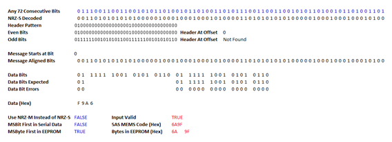
I put together an Excel spreadsheet which can decode the 5AS data stream just to prove all of the above concepts and to allow me to work out the possible MEMS codes and EEPROM bytes for each of my immobilisers. I felt that the chances of making a mistake decoding them all by hand were too high, and even a 1-bit error could lead me down a blind alley. The spreadsheet allows you to enter any 72 consecutive bits of data from the data stream, not necessarily starting at the start of a message, and implements all of the logic above for decoding NRZ-S or NRZ-M, determining the odd and even bit streams, determining the offset to the start of the message and decoding the hexadecimal 16-bit data word transmitted and the corresponding EEPROM bytes. It also allows any of the unknown encoding options listed above to be selected.
For completeness I also added a tab which performs the complementary encoding, taking the two consecutive EEPROM bytes and generating the MEMS code and 72-bit repeating sequence transmitted. This allowed me to test the decoder functionality above to make sure I hadn’t made any mistakes coding it.
Note that when encoding, there is a further assumption to be made. Each “0” bit causes the output state to toggle, each “1” bit keeps the previous output state, but if the very first bit to be encoded is “1”, what is the output state? There is no previous output state to maintain. So we have to make an assumption about the initial output state of the encoder.
The two possible initial states give two different encoded output bit sequences, both of which correctly encode the same message and both of which can be decoded correctly and identically. For MEMS codes which have an odd number of transitions (those which repeat every 72 bits), we see both of these bit sequences in the streamed data, alternately beginning with “01110” and “10001”. However, for MEMS codes which have an even number of transitions (those which repeat every 36 bits), we only ever see one of these bit sequences in the streamed data, always beginning with “01110”. Using the spreadsheet above, I found that assuming an initial “1” state always produced the “01110” sequence which is seen in the 5AS output; assuming an initial “0” state always produced the “10001” Sequence which is not seen in the 5AS output in the initial message or in any message with an even number of transitions, so it was clear that the encoder in the 5AS assumes an initial state of “1”.
Unfortunately, an initial state of “1” generates sequences beginning with “01110” irrespective of whether NRZ-S or NRZ-M encoding is used, so this gave no clues as to the correct assumption here.
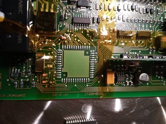
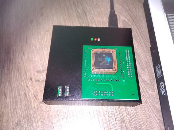
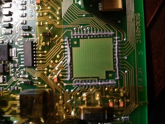
So now that I had a good idea what I was looking for in the EEPROM data it was time to desolder the microcontroller chip and have a look at it in a programmer to see if I could find the MEMS codes I had decoded. This was a lot easier than when I had previously desoldered memory chips from the ECU as the circuit board was quite conventional, rather than being a large metal heatsink. I again used a temperature controlled hot air gun from a solder rework station. In order to protect surrounding components from becoming detached, I masked the area immediately around the microcontroller with high temperature Kapton tape. This provided both a degree of heat shielding and some mechanical adhesion and support to prevent parts from moving if the solder did melt.
The
microcontroller was then removed quite easily using a reasonably high flow of
350°C air. I wanted to use the highest temperature I could as this would result
in removing the component in the least time, which somewhat counter-intuitively
means that the chip internals do not get as hot during the process as when
using cooler air. Anything over 400°C risks scorching a fibreglass PCB so 350°C
seemed to be a good compromise.
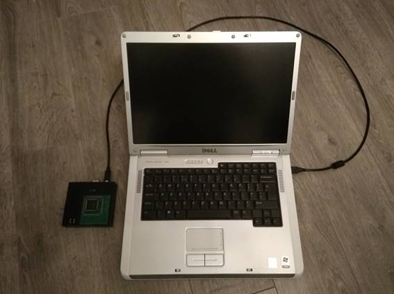
The
programmer I chose to use was an XPROG-M - or more accurately I believe a
Chinese clone of an XPROG-M with some very dodgy software indeed (it would only
work on Windows XP or Windows 7 32-bit which cannot be on a virtual machine, it
came with instructions saying you must disable your virus scanner and sure
enough when I tried to install it without doing so the scanner identified
various threats, and instructions that you must diasable your internet
connection as presumably if you don’t, it will download updates up the proper
official software without all the hacks which would stop it working). Because I
was only using this for my own hobby use and because I couldn’t actually find
anything else at price that was at all reasonable for single hobby use which
was capable of defeating the security protection systems on the microcontroller
I persevered with it - on an old, no longer required XP laptop which I
disconnected from everything else and would be quite happy to wipe clean once I
was finished!
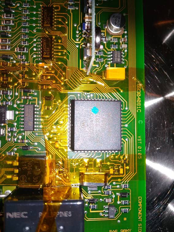
The
programmer comes with an adapter for the MC68HC05B16 with a convenient PLCC52
socket so I didn’t need to solder the it to the board. Here is a picture of the
microcontroller mounted in the adapter on the programmer:
After
jumping through all of the required hoops specified in the instructions, which
included installing a very old Chinese language copy of Adobe Reader (oddly the
software won’t even launch if you uninstall or update this) and importing a
file of registry hacks, the software actually loaded and worked well. First of
all I selected the device (Type, “MCU/MPU”, Subtype “Freescale HC05”, Device
“MC68HC05B4/B6/B8/B16/B32”) which reassuringly listed mask code 0D60J as being
supported.
Then
I created a new project and clicked “Read”. It worked through “Check device…”

“Initialising
device …”
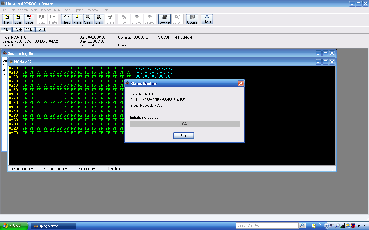
“Bypass
security” - this is where it had determined that the security bit was set
preventing a switch to “non user” mode and set up the clock glitching attack to
effect the switch using “back door” methods. It only took a couple of seconds.

And
finally repeated the whole cycle again, verifying the read.
This
left me with a dump of the EEPROM data from the microncontroller, displayed in
hexadecimal format, which I saved to a .BIN (raw binary) file. The
microncontroller has 256 bytes of EEPROM, starting at address 0x100. So in the
data displayed, offset 0x00 in the data file is actually at address 0x100 in
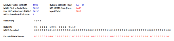
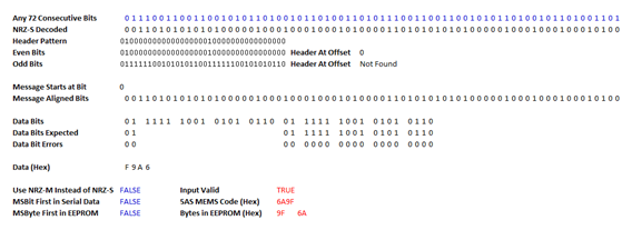
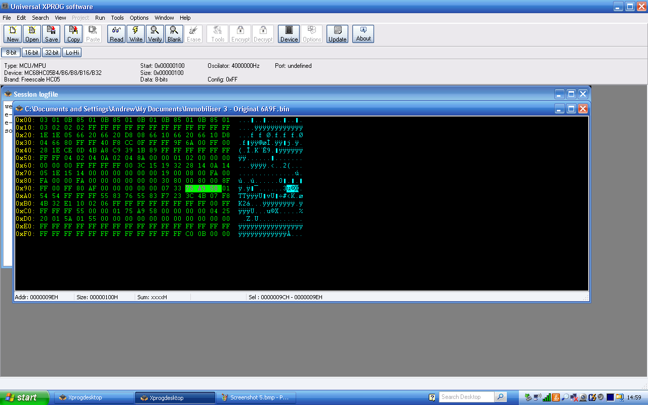
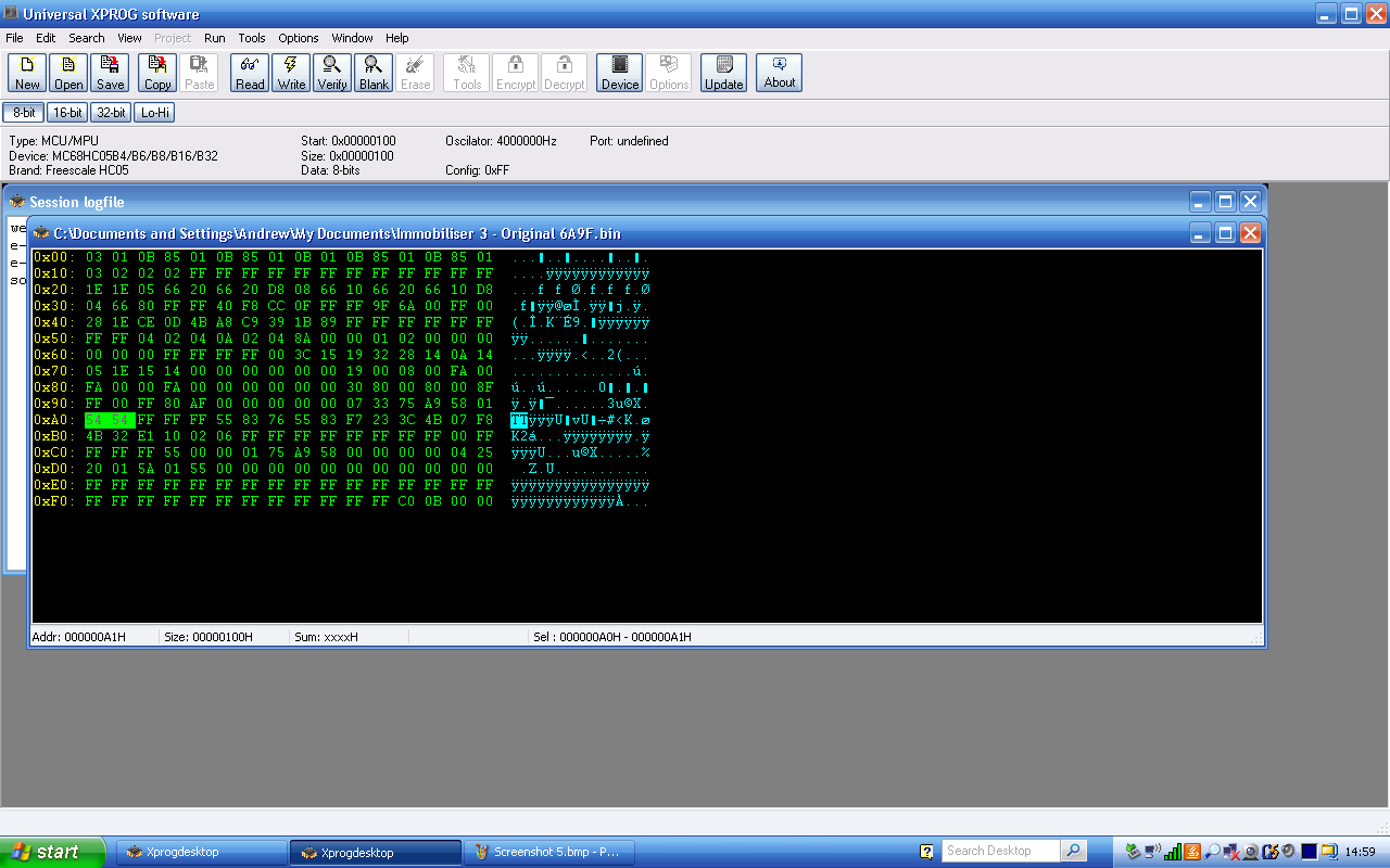
the address space of the microcontroller etc. And sure enough … at offset 0x3B
(address 0x13B) there were the two consecutive bytes 0x9F, 0x6A of the MEMS
code 6A9F which I had decoded for this immobiliser! The only issue was that
they were in reverse order, which means that my assumption that the storage
order would follow the Big Endian convention of the processor was wrong.

So
I updated my encoder and decoder spreadsheets with FALSE for “MSByte First in
EEPROM” as shown below. I then repeated the whole procedure with a couple of
other immobilisers just to convince myself and in each case the MEMS code which
I decoded from the bit stream appeared at these same addresses in the EEPROM in
the same format, which they did. This effectively confirmed all of the other
assumptions I had made and my method for decoding the immobiliser data stream,
so I was now sure which bytes I would need to preserve in order to retain the
original MEMS code when copying the EEPROM settings from one immobiliser to
another - or conversely, which bytes to change if I wanted to copy the MEMS
code from one immobiliser to another so that the ECU would see them as the same
unit.
From
this site: https://blackbox-solutions.com/help/SM034.html
I was also aware that the alarm serial number printed on the label on the case
should also be found in the EEPROM somewhere. In this case the serial number
was 5810549 (decimal) …
Which
is 0x58A975 in hexadecimal, and this number also showed up at offset 0x9C
(address 0x19C) … unusally stored as a 3-byte number (neither of the bytes
either side were 0 as would be expected if it was in a 4-byte format) and again
with the least significant byte first (75, A9, 58) confirming that this seemed
to be the order in which the microcontroller software was storing the bytes of
integers. A 3-byte number is very unlikely to be written by any of the
microcontroller instructions directly (I may be wrong, I haven’t studied the
HC05 family instruction set in detail), so my guess is that the sofware is
writing multi-byte integer values explicitly one byte at a type, in Little
Endian order with the least significant byte first.
The
EKA code was also recognisable at offset 0xA0 (address 0x1A0), with a length of
two bytes. The EKA is an Emergency Key Access code which, on a Rover, allowed
the immobiliser to be disarmed through a sequence of turns of the key in the
driver’s door lock, and was of particular interest to me for some other work
I’m doing. This is a four digit code, each digit being 1-9. Each byte here is
storing one digit in the upper four bits and one digit in the lower four bits.
The EKA is readable and writable using my T300+ key programmer, and I was able
to match up the codes in the different immobilisers at this location. In this
case the code was 5-4-5-4. With this particular immobiliser it’s hard to tell
which order the bytes are stored in as theey are both the same (0x54) due to
the repetitive code, but on another immobiliser which showed an EKA code of
2574 on the T300+, the bytes were 0x25, 0x74 which means the first two digits
of the EKA code are stored in the first byte and the second two digits of the
EKA code are stored in the second byte. If you think of the EKA code as being a
hexadecimal integer but only using the digits 1-9, this is actually the reverse
of the order used for other integers I found with the most significant byte
first.
Somewhere
in the data there should also be the week and year of build, but I couldn’t see
anything obvious. They could be encoded in so many ways. There were no
consecutive integers corresponding to the week and year, but it could just be a
number of weeks since a given date etc. I didn’t waste a lot of time looking
for it for now. I don’t really need to be able to reset the date of
manufacture; it’s on the label on the cover anyway. There should also be a
count of the number of matched key fobs and the corresponding key IDs; these
are things that I will come back to hunting for later. Even though my T300+ key
programmer is easily able to match keys to immobilisers this does require all
of the keys to be physically present, and sometimes I get involved with helping
people with immobiliser issues remotely so an option to match a key directly in
memory could be useful.
So
the next question I needed to answer was this: Is there any kind of checksum
protection on the EEPROM data? Given that the EEPROM is also used to hold alram
trigger event logging information and updated at run time, it seemed unlikely,
but before I went any further I decided to check that I was able to make
changes to the EEPROM contents and still get the immobiliser working properly
again.
At
this point I decided to avoid making mistakes when editing the files, I would
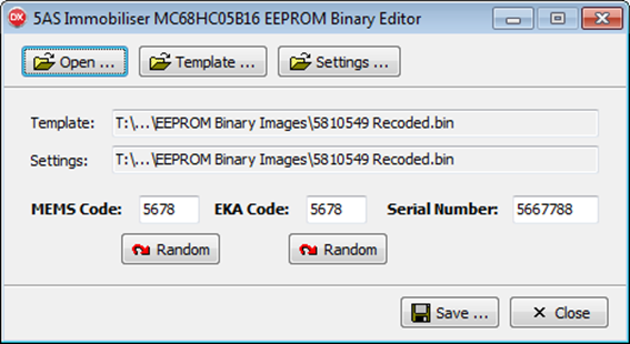
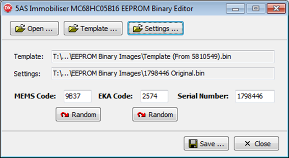
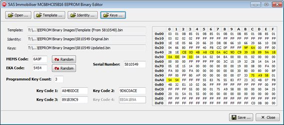
put together a little software utility for editing 5AS .BIN files:
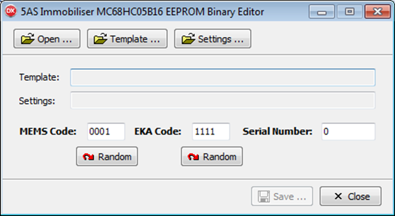
This
allows me to open a .BIN file dumped from an immobiliser EEPROM and manually edit
the identified settings, or to load one .BIN file as a template and then load
the settings from another and save the merged file. So, using the above utility
I updated the .BIN file downloaded from one of the immobilisers and changed the
MEMS code and EKA code to 5678 and the serial number to 5667788, and used the
XPROG-M programmer to upload this back to the microcontroller to see whether it
still worked properly, whether the transmitted data stream matched my encoding
of the new MEMS code 5678 as expected and whether the ECU could then be matched
to this new code.
Before
attempting to solder the microcontroller chip back onto the circuit board I
cleaned up the solder pads on the circuit board with solder mop braid and then
a good clean with pure isopropyl alcohol. Then I masked around the
microcontroller with high temperature Kapton tape and laid a “sausage” of
solder paster long each set of pads. It didn’t matter that the paste bridged
across the pads as the flux in the solder paste would allow it to pull back
into the terminals and solder pads under surface tension once it melted.
I then used hot air at 350°C and a moderate flow rate, working along each side
until the chip was neatly soldered back into place. I inspected the finished
soldering carefully with a jeweller’s loupe to make sure there were no dry
joints, bridges of solder between pins or misaligned contacts but all looked
good.
I then let everything cool back down to room temperature before applying power as the chip was well outside its allowed operating temperature range once I had finished soldering and powering it up in this condition could do irreversible damage.
Time for testing and the immobiliser came to life straight away, I matched it to a couple of key fobs and an ECU using the T300+ key programmer on my key programing interface and everything worked exactly as expected. The ECU was perfectly happy with the new signal but need to be matched again, which was a promising sign that I had given the immobiliser a new but valid MEMS code. This confirmed that there were no checksums to update, at least none which covered the MEMS code, EKA code and serial number areas of the EEPROM.
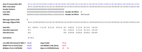
Once again I hooked up an oscilloscope to Pin 9 of the immobiliser to record the communications between the 5AS and the ECU. Here is the captured encoded waveform:
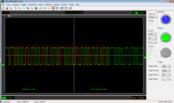
And here is the decoding of the above signal in the spreadsheet, confirming that it is a valid signal representing the new MEMS code of 5678 which I had programmed into the EEPROM:
So far, so good. I had proved that I was able to find all the relevant settings in the EEPROM data and update them on a single ECU. But having proved the concept by updating a single ECU, the next task was to check that the EEPROM data could be copied between immobilisers without causing any issues. This would only be possible if the Lucas 53873824 stamping on the microcontroller chip did indeed mean that the software was identical; or at least the software was sufficiently similar between the immobilisers which I had that it used the same memory layout in EEPROM for all of the parameters that impacted on features used in the Caterham installation. This was the ultimate goal, to allow me to copy my ideal settings from one immobiliser to others whilst preserving their unique identities. It seems such a long time ago that I set out on that mission that it’s easy to forget what the original objective was!
Using my software utility, I loaded the template .BIN file taken from the immobiliser whose behaviour I wanted to copy and updated it with the MEMS code, EKA code and serial number taken from the .BIN file downloaded from one of the other immobilisers, which was not showing the passive arming behaviour that I wanted.
I then burned it back to the microcontroller of the second immobiliser, soldered it back into place and tested as before. Bingo! The second immobiliser new displayed all of the same passive arming behaviour as the first but still retained its unique IDs. All of the other configuration options and behaviours seemed completely consistent too as expected.
I repeated this for each of my spare immobilisers, with complete success every time. Mission accomplished.
Well, not quite …
For completeness, I said earlier that I wanted to try to work out the location and layout of the key fob coding data in order to allow me to copy the key fob programming from one immobiliser to another. I didn’t have any information on the key codes so my plan of attack on this one was:
· Dig out a few spare keys (I have a large bag of key circuit boards, all remanufactured, testing and working, but that’s another write-up!) and label them up as A, B, C, D and E.
· Program one immobiliser to accept keys A, B, C and D (the immobiliser can accept a maximum of 4 key fobs at a time).
· Remove the microcontroller and download the EEPROM contexts.
· Avoid triggering any alarm events as far as possible as these could update other memory locations with logging which might confuse the search.
· Put it all back together and program it to accept keys B, D and E.
· Remove the microcontroller and download the EEPROM contexts.
· Compare the two files and try to identify changes consistent with:
o The number of keys changing from 4 to 3.
o Two of the original key codes (B & D) still being present but appearing in different positions (corresponding to slots 2 and 4 in the first case and 1 and 2 in the second case).
o A new key code being added (E).
· Once I had a theory, test it by making predictions about the memory contents I would expect to see with other key combinations and then setting these up and inspecting as above.
I figured this pattern would give me a good chance of spotting what was what.
This plan would involve repeatedly soldering and desoldering the microcontroller on one immobiliser quite a few times. I’m really not sure how well the chip and the circuit board will take the punishment but there’s only one way to find out. I think by the time I’ve finished this process, that one immobiliser will be clearly marked as for experimentation only and not to be used in a car as I have no idea how the reliability may have been affected. On the plus side, I’m getting quite practised at soldering and desoldering these chips now and can do it in a few seconds, usually getting it right first time, so the heat exposure involved is going down.
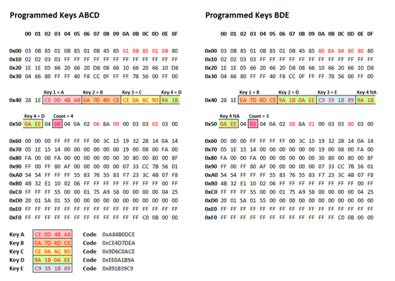
Here is the data I got. I have highlighted in red the bytes which changed between the two data sets.
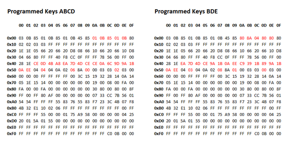
What can be seen here? Well there is a block of changes in the middle starting at offset 0x42 which makes a lot of sense and looks exactly like the key coding data I was expecting. There are several other bytes which have also changed which I don’t understand, but these are probably just event logging, key rolling code counters or something like that. Since the block of changes in the middle were exactly what I was expecting, I went with the theory that these were exactly what they appeared to be and the rest was just irrelevant noise.
In the first data set we see four blocks of four bytes each, which appear to be the key codes for keys A, B, C and D. Assuming these are in Little Endian format as normal with the least significant bytes first (and to be honest it makes no difference, it’s just a matter of convention how we choose to make key codes out of these as the codes are never seen anywhere else, so as long as we are consistent it will all work) they give 32-bit codes 0xA84B0DCE, 0xCE4D7DEA, 0x9D6C0ACE and 0xEE0A1B9A for keys A, B, C and D. We also see at offset 0x53 a count of 4 keys.
In the second data set we see in the same four blocks of addresses the key codes for keys B and D, followed by a new key code 0x891B39C9 which must be key E. After this is the key code for key D again. The fourth key code slot is not used as the count at 0x53 specifies that 3 keys are matched; it looks as though the data has simply not been overwritten by a new key so the old key D data remains.
So on that basis, the writing the following data should leave the immobiliser matched to keys A, C and E only:
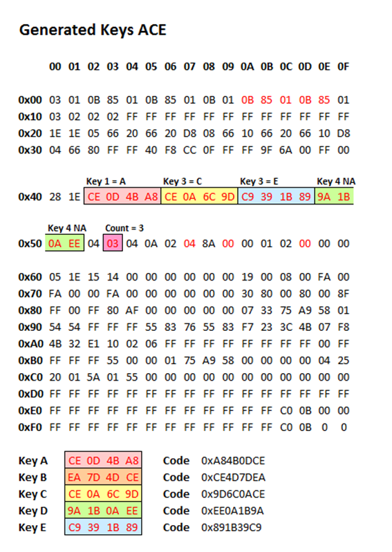
I extended my software utility to include the key count and codes (and quite a bit else, such as full display, highlighting and editing of all of the binary data as you will see in the picture below) and used this to prepare a data set similar to the one shown above, with a key count of 3 and the key codes for keys A, C and E only:
I then uploaded this test .BIN to the microcontroller and tested the immobiliser. As expected, keys A, C and E now worked. But there was a catch, in that keys C and E worked immediately, key A did not. Eventually after pressing it many, many times (I didn’t count) it started working. So I can only assume that as I suspected earlier, some of the other bytes which changed were used by the rolling code generation and stored some kind of internal state of the key, and my changes had left the sequence counts in the immobiliser and key badly out of synchronisation and the key needed to roll right around a full sequence until it dropped back into line.
It seems logical that such key states would be stored somewhere close to the key codes in the same block of EEPROM memory, so my guess at this stage would be that the five changed bytes at offset 0x0A would still just be some kind of event recording and that the three changed bytes at offsets 0x57, 0x59 and 0x5D would be key state information. There three bytes are spaced out by 2 bytes then 4 bytes. I would also guess at this stage that there are actually four bytes representing the four keys in sequence, equally spaced by 2 bytes each, at offsets 0x57, 0x59, 0x5B and 0x5D - and that the byte at 0x5B just happened to take the same values in the two data sets I was comparing, which is not unlikely as they all seem to be small numbers. It further made sense as the last of these was set to 0 in the case where there were only three keys programmed, so my guess would be that this state information is cleared down at the start of the programming process and updates as the key signals are received.
However, I don’t think I really have enough information about all of this works to make it worthwhile trying to copy the key state information. So I think for now I will live with the fact that keys may need to be clicked quite a few times to resynchronise the first time they are used after programming directly in EEPROM. After all, I should imagine that 99% of the keys I will ever program will be done through the T300+ and key learning mode on the immobiliser where the problem does not arise.
This work has allowed me to achieve everything practical I set to do with the immobiliser programming. In addition to fully understanding the key data, there are still a few ideas I’d like to play with in the future. For example, I have been told that MEMS codes 0x0000, 0xF0F0 and 0xFFFF are not allowed, but as far as I can see they don’t break the coding scheme so I can only assume that they have some special meaning in the ECU. As a complete guess at the moment … I wonder if the ECU uses one these codes for “factory mode” (where it learns the code of the first immobiliser it gets a valid signal from)? And if so, can I trick an ECU to go into factory mode by putting one of these special codes into an immobiliser and then getting the ECU to learn the code from it? Probably not … but worth a try!
If anyone has any inside info on the Lucas 5AS that might help me understand I’d love to hear from them please. I could then expand this for future reference.